In the age of artificial intelligence, the ultimate measure of the success of an AI product is how much it can improve the efficiency of our lives. As AI technology moves from the cloud to the edge, the engineering problems that need to be optimized will become more complex. Effective evaluation before chip design becomes increasingly important for the ultimate success of the product. However, due to the complex nature of AI chip application scenarios, the industry needs correct and professional evaluation tools.


One of the conundrums of the AI industry:
AI chips can't keep up with the speed of algorithms


As early as 2019, Stanford University reported that the speed of AI's demand for computing power is faster than the development speed of chips. "Before 2012, the development of AI followed Moore's Law very closely, and the computing power doubled every two years, but after 2012, the computing power of AI doubled every 3.4 months."
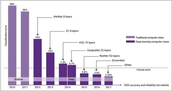
When the computing power of general-purpose processors cannot keep up with the needs of AI applications, dedicated processors for AI computing are born, which is often referred to as "AI chips". Since 2015, AI algorithms have surpassed human scores in visual recognition, and the industry has paid more attention to AI chips, which has also driven the development of related IP technologies, accelerated the speed of next-generation processors and memories, and achieved higher bandwidth interfaces. , so as to keep up with the pace of AI algorithms. Figure 1 shows the visible reduction in AI typical error rates since the introduction of backpropagation and modern neural networks in 2012, combined with NVIDIA’s heavy-duty compute GPU engine.

Figure 1: After the introduction of modern neural networks in 2012, AI classification errors decreased rapidly, lower than human error rates since 2015
As AI algorithms become more complex and cannot be executed on SoCs designed for consumer products, they need to be compressed using pruning, quantization, and other techniques to align and compress, reducing the amount of memory and computation required by the system, but at the expense of accuracy. So there is an engineering challenge: how to implement compression techniques without compromising the accuracy required for AI applications?
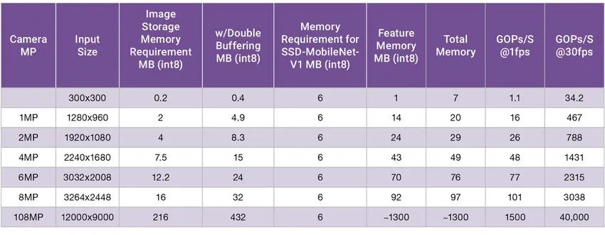
In addition to the increasing complexity of AI algorithms, the amount of data required for inference has grown dramatically due to the increase in input data. Figure 2 shows the memory and computation required for the optimized vision algorithm. The algorithm is designed to have a relatively small 6MB memory footprint (memory requirement of SSD-MobileNet-V1). In this particular example, we can see that the memory requirement in the latest image capture has increased from 5MB to over 400MB as the pixel size and color depth have increased.
Currently the latest Samsung mobile phone CMOS image sensor camera supports up to 108MP. In theory, these cameras could require 40 TOPS of performance at 30fps and more than 1.3GB of RAM. However, the technology in the ISP and the specific area in the AI algorithm cannot meet these requirements, and the 40 TOPS performance cannot be realized on the mobile phone. But this example shows the complexities and challenges of edge devices and is also driving the evolution of sensor interface IP. MIPI CSI-2 has a dedicated area to address this, and MIPI C/D-PHY continues to increase bandwidth to handle the latest CMOS image sensor data driving hundreds of millions of pixels.

Figure 2: Memory change test of SSD-MobileNet-V1 as input pixels increase
Today's solution is to compress AI algorithms, compress images, which makes chip optimization extremely complex, especially for SoCs with limited memory, limited processing capacity and small power budgets.


AI industry problem 2: AI chip evaluation faces challenges


AI chip makers usually do some benchmarking of their chips. There are many different metrics for SoCs today. First, tera operations per second (TOPS) is a primary indicator of performance, and this data provides a clearer picture of chip capabilities, such as the type and quality of operations the chip can handle. Again, inferences per second is a primary metric, but frequency and other parameters need to be understood. Therefore, additional benchmarks have been developed in the industry to help evaluate AI chips.
Both MLPerf/ML Commons and AI.benchmark.com are tools for standardized benchmarking of AI chips. Among them, ML Commons mainly provides measurement rules related to chip accuracy, speed and efficiency, which are very important for understanding the chip's ability to process different AI algorithms. There is a trade-off between the degree of compression. In addition, ML Commons provides common datasets and best practices.
The Computer Vision Lab in Zurich, Switzerland also provides benchmarks for mobile processors and publishes their results and silicon requirements and other information to support reuse. Includes 78 tests and over 180 performance benchmarks.
DAWNBench at Stanford University provided support for the work on ML Commons. These tests address not only AI performance scoring, but also the total time it takes for a processor to perform AI algorithm training and inference. This addresses a key issue of chip design engineering goals, which is to reduce the total cost of ownership, or total cost of ownership. AI processing time, which determines chip ownership for cloud AI leasing or edge computing, is more useful for an organization's overall AI chip strategy.
Another popular benchmarking method is to utilize common open source graphs and models, but these models also have some drawbacks. For example, the ResNET-50 dataset is 256x256, but this is not necessarily the resolution that might be used in the final application. Second, the model is older and has fewer layers than many newer models. Third, the model can be manually optimized by the processor IP vendor, but this does not represent how the system will perform with other models. In addition to ResNET-50, there are a large number of open-source models available through which recent advances in the field can be seen and provide good metrics for performance.
Finally, custom graphics and models for specific applications are becoming more common. Ideally, this is the best way to benchmark an AI chip and properly optimize it to reduce power consumption and improve performance.
Because SoC developers have different goals, some are for high-performance applications, some are for lower-performance areas, some are general AI, and some are ASIC. For SoCs that don't know which AI model they need to optimize by, a good mix of custom models and openly available models is a good indicator of performance and power consumption. This combination is most commonly used in the market today. However, the emergence of the newer benchmarking standards mentioned above seems to be somewhat relevant in comparisons after SoCs have entered the market.


Evaluation before edge AI chip design is especially important


More and more data computing is now happening at the edge, and given the complexity of edge optimization, today's AI solutions must co-design software and silicon. To do this, they must utilize the right benchmarking techniques, and must be supported by tools that allow designers to accurately explore different ways of optimizing a system, SoC, or semiconductor IP, investigating process nodes, memories, processors, interfaces, and more.
In this regard, Synopsys provides domain-specific tools for simulating, prototyping, and benchmarking IP, SoCs, and broader systems.
First, Synopsys HAPS® prototyping solutions are often used to demonstrate the capabilities and trade-offs of different processor configurations. The tool is able to detect when, in addition to the processor, the bandwidth of an AI system starts to become a bottleneck? What is the optimal bandwidth for sensor input (via MIPI) or memory access (via LPDDR) for different tasks?
Again, the Synopsys ZeBu® simulation system can be used for power simulation. ZeBu Empower can take real software workloads for AI, 5G, data center and mobile SoC applications and complete power verification cycles in hours. This simulation system has been shown to outperform simulation and/or static analysis of AI workloads.
Users can also explore the system level of SoC designs through Synopsys' Platform Architect. Originally used for memory, processing performance and power exploration, Platform Architect has been increasingly used to understand system-level performance and power consumption for AI. Using pre-built LPDDR, ARC processor models for AI, memory, and more, sensitivity analysis can be performed to determine optimal design parameters.
Synopsys has an experienced team developing AI processing solutions from ASIP Designer to ARC processors. A proven portfolio of foundational IP, including memory compilers, is widely used in AI SoCs. Interface IP for AI applications ranges from sensor inputs to I3C and MIPI, to chip-to-chip connectivity via CXL, PCIe and Die to Die solutions, and networking capabilities via Ethernet.


Summarize


Software and silicon co-design is a reality, and choosing the right tools and expertise is critical. Synopsys is leveraging expertise, services, and proven IP to provide customers with the best-fit approach to optimizing AI chips under changing circumstances.
author of this article
Ron Lowman, IP Strategic Marketing Manager, Synopsys
*Disclaimer: This article was originally written by the author. The content of the article is the author's personal opinion. The reprint of Semiconductor Industry Observation is only to convey a different point of view. It does not mean that Semiconductor Industry Observation agrees or supports the view. If you have any objection, please contact Semiconductor Industry Observation.
Today is the 3120th content shared by "Semiconductor Industry Watch" for you, welcome to pay attention.
Recommended reading
★ Japan's power semiconductors, another step ahead
★ AMD's market value surpasses Intel's, the beginning of a new era
Semiconductor Industry Watch

" Semiconductor First Vertical Media "
Real-time professional original depth
Identify the QR code , reply to the following keywords, read more
Wafer|Integrated Circuits|Devices|Automotive Chips|Storage|TSMC|AI|Packaging
Reply Contribution , see "How to become a member of "Semiconductor Industry Watch""
Reply to search , and you can easily find other articles you are interested in!

