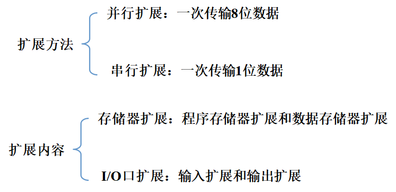
The internal memory and I/O port resources of the microcontroller are limited, and external expansion is required in most cases .
1. Extension methods and content
Second, the bus introduction
The typical structure of the parallel expansion of the microcontroller is the bus structure.
The expansion components are connected with the single-chip microcomputer through the bus, which is equivalent to that each component in the system hangs on the bus, and uses the bus to communicate with the CPU in time-sharing.
When a component is selected, it can be read, written and controlled, while other components and the bus are in a "high-impedance state", which is equivalent to disconnecting from the bus.
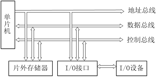
The three-bus construction method of the single-chip system is as follows:
The P0 port line is used as the data bus/low-order address bus 4, and the P2 port line is used as the high-order address bus;
Use function pins to form a control bus.
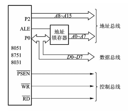
Use P0 port line as data bus/low address bus: first use P0 port line as address bus, send the lower 8-bit address to the latch, and the latch provides it to the system; then use P0 port line as data bus to read and write data, so that the lower 8-bit address signal of the address bus and the data bus share the P0 port line without conflict.
Use P2 port line as high-order address bus: P2 port line can provide up to 8-bit high-order address, plus the low-order 8-bit address provided by P0 port line, it can provide up to 16-bit address, which can make the addressing range of the microcontroller system up to 64KB .
Use function pins to form a control bus: RD (P3.6 pin) and WR (P3.7 pin) are used as read and write strobe signal lines; ALE is used as address latch signal line to cooperate with P0 port to realize time-sharing Multiplexing; PSEN is used as the off-chip program memory to read the strobe signal line; EA is used as the selection signal of the on-chip and off-chip program memory.
Basic operation control of memory, including chip select control and read and write operation control.
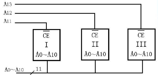
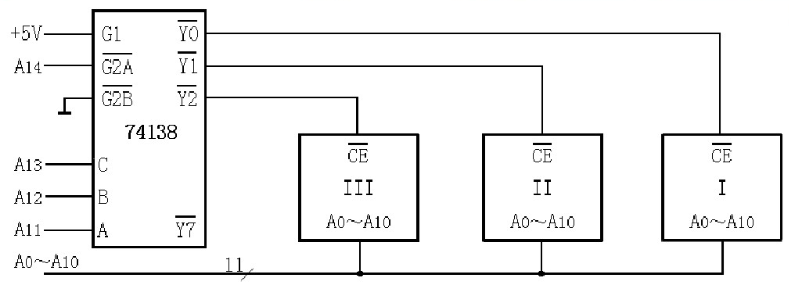
Line selection method: Status address lines (A0~A10) realize on-chip addressing, and high-order address lines (A11~A13) realize chip selection. The line selection method is simple to connect, but the address space is discontinuous, which is suitable for the case where the expansion capacity is small and the number of chips is small.
Decoding method: Convert the high-order address line into a chip select signal through a decoder. The decoding method can effectively use the storage space, and the address is continuous, which is suitable for expansion under multi-chip. Commonly used decoder chips are 74138 and so on.
3. Storage expansion
Address line: The address is provided by the P0 and P2 ports. In the address lines (A0-A15) of the ROM, the lower 8 bits A0-A7 are connected with the P0 port through the latch 74LS373, and the upper 8 bits A8-A11 are directly connected with the P2.0-P2.7 of the P2 port.
Data line: The 8-bit data line of the off-chip ROM is directly connected to the P0 port of the microcontroller.
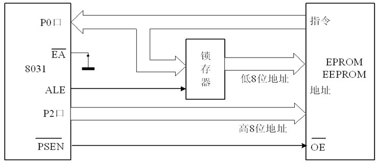
Control line: When the CPU executes the program instructions stored in the ROM, the instruction fetch stage is to read the ROM. The read operation control lines are as follows:
Address latch signal ALE, chip select signal CS, read strobe signal OE, selection control signal EA of off-chip program memory
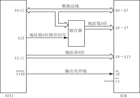
Address latch signal ALE: The ALE pin of the single-chip microcomputer is connected to the latch enable terminal G of the latch, which is used for the single-chip microcomputer to give a latch signal of the lower 8-bit address when reading instructions from the off-chip ROM.
Chip select signal CS: active low. If only one program memory chip is expanded in the system, the chip selection terminal can be directly grounded, so that the chip is always valid. If multiple chips are expanded at the same time, the chip selection work needs to be completed by the line selection method or the decoding method.
Read strobe signal OE: active low. This pin is connected to the off-chip ROM read strobe signal terminal PSEN of 8051. When accessing off-chip program memory, as long as there is a negative pulse at this end, the instruction or data can be read from the ROM.
The selection control signal EA of the off-chip program memory: when the EA pin is connected to a high level, the CPU only accesses the program memory inside the microcontroller and executes the instructions in the internal program memory, but when the program storage exceeds the maximum capacity of the internal program memory, It will automatically switch to execute the program in the external program memory of the microcontroller. When the input signal pin is connected to low level (grounded), the CPU only accesses the external program memory and executes the instructions in the external program memory.
When executing the off-chip ROM read instruction, the operation sequence of the microcontroller automatically:
(1) First, the 16-bit address is given by the PO port and the P2 port, and then the falling edge of ALE informs the latch to latch the lower 8-bit address of the P0 port;
(2) The low level of PSEN makes the off-chip ROM valid;
(3) According to the address provided by the latch and the P2 port, the instruction is taken out and sent to the P0 port, and the P0 port is read into the microcontroller for execution.
In the above process, the read and write signal terminals WR and RD of the data memory RAM are always in a high level state, which isolates the RAM from the bus.
Fourth, the control program
Write a program according to the circuit in the figure below to display a total of 10 digits from 0 to 9 in a circular display with a digital tube.
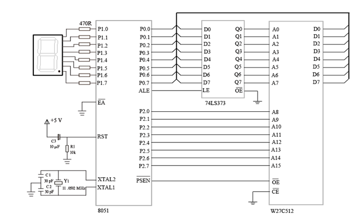
unsigned char led[]={0xC0,0xF9,0xA4,0xB0,0x99,0x92,0x82,0xF8,0x80,0x90};//字型码int main(void){unsigned char i;while(1){for(i=0;i<10;i++)//循环显示10个数字{P1=led[i];delay();//延时一段时间}}}void delay()//延时函数{int i,j;for(i=0;i<3000;i++)for(j=0;j<5;j++);}
5. Data storage expansion
The expansion of the data memory RAM mainly uses the following three control signals:
ALE: low 8-bit address latch control signal, usually connected to the LE pin of the address latch;
WR: External RAM write signal, active low, connected to the WE pin of the data memory;
RD: External RAM read signal, active low, connected to the OE pin of the data memory.
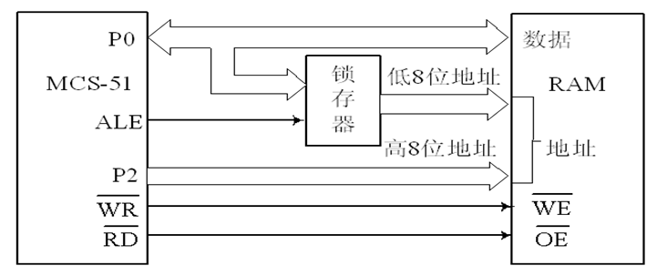
When executing off-chip RAM read and write instructions, the automatic operation sequence of the microcontroller is similar to that of reading ROM:
(1) First, the 16-bit address is given by the PO port and the P2 port, and then the falling edge of ALE will latch the lower 8-bit address of the P0 port;
(2) When reading data, RD appears low level, WR appears high level, so that the off-chip RAM is valid, and according to the address provided by the latch and P2 port, the data is taken out and sent to the P0 port, and the P0 port is read into the microcontroller. .
(3) When writing data, first load the data into the P0 port, then the RD pin appears high level, and the WR pin appears low level, so that writing off-chip RAM is valid, and according to the address provided by the latch and P2 port Write the data on the P0 port into the off-chip RAM.
6. Program example
Write a program according to Figure 8-4 to store the font code of 10 digits from 0 to 9 displayed by the digital tube into 6264, and then read the font code from 6264 cyclically and send it to the digital tube for display.
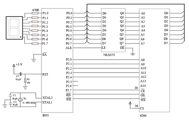
unsigned char led[]={0xC0,0xF9,0xA4,0xB0,0x99,0x92,0x82,0xF8,0x80,0x90};//字型码int main(void){unsigned char i;for(i=0;i<10;i++)//存储10个数字字型码XBYTE[0x8000+i]=led[i];while(1){for(i=0;i<10;i++)//循环显示10个数字{P1=XBYTE[0x8000+i];delay();//延时一段时间}}}void delay()//延时函数{int i,j;for(i=0;i<30000;i++)for(j=0;j<5;j++);}
For the expansion of the functions of the input/output ports, a simple TTL circuit or a MOS circuit can be used, or a programmable interface chip with a more complex structure can be used.
The MCS-51 single-chip computer uniformly addresses the I/O port and the off-chip RAM, and the two together use the same 64KB externally extended address space. Therefore, the input and output instructions of the I/O port are also the data of the off-chip data memory. read/write commands.

Simple input expansion is mainly realized by three-state data buffer, and the purpose is to enable the gated input device to exclusively input data to the single-chip microcomputer from the data bus, while the non-gated device is isolated from the data bus. Commonly used three-state data buffer chips are 74LS244 and so on.
The simple output expansion is mainly realized by three-state data latch, the purpose is to enable the single-chip microcomputer to output data to the gated device through the data bus, and the non-gated device is isolated from the data bus. Commonly used tri-state data latch chips are 74LS273 and so on.
The 8051 single-chip microcomputer uses 74LS373 and 74LS245 to expand the I/O ports, respectively connect the light-emitting diode and the DIP switch.
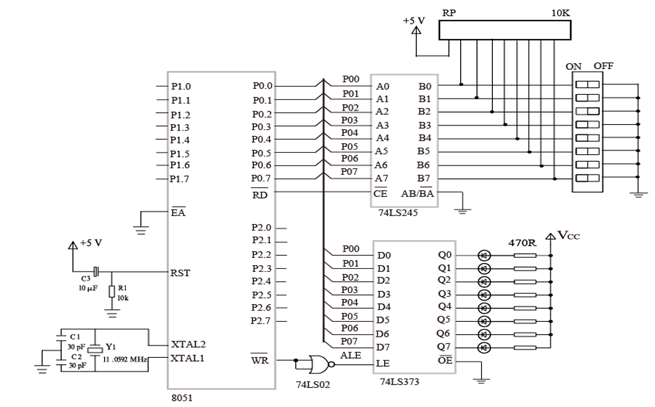
int main(void){unsigned char temp;while(1){temp=PORT; //读存储单元操作,即通过74LS245获取开关数据PORT=temp; //写存储单元操作,即通过74LS373用开关数据控制发光二极管}}
Due to the recent changes in the push rules of the WeChat public platform, many readers reported that they did not see the updated articles in time. According to the latest rules, it is recommended to click "recommended reading, sharing, collection", etc. to become frequent readers.
Recommended reading:
Please click [Watching] to add chicken legs to the editor
